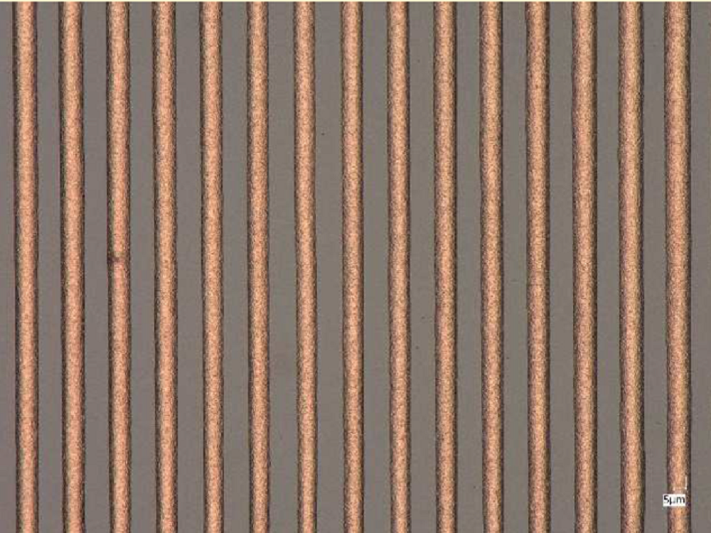
● Printable by gravure offset printing which enables fine-pitch trace down to L/S=7/12μm.
● < 10-5 Ω-cm order volume resistivity of at <150℃ by using formic acid reflow oven.
0
#Conductive paste #High density interconnect #Fine trace #Copper nanoparticles #Low temperature sintering #Gravure offset printing
Potential Applications
● Package substrate trace/Interposer trace/High density interconnect
● Package substrate bump/Interposer bump
● Display trace
● Electrodes of passive components
General Characteristics
| Test item | Developed product |
|---|---|
| Viscosity (Pa-s) | 10 to 100 |
| Recommended curing conditions | 150°C x 30 min in N2 + formic acid |
| Volume resistivity (Ω-cm) | 1.0 x 10⁻⁵ |
| Printing method | Gravure offset, screen |
| Storage conditions | Refrigeration |
*All values are representative.
Printability
● Gravure offset printing
Cooperation: Komori Corporation
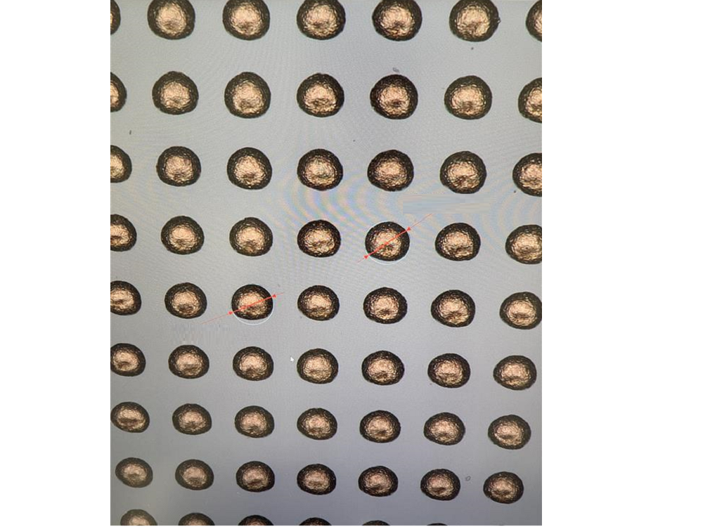
▼φ15μm bumps printed by gravure offset printing
▼L/S=7/12μm copper traces printed by gravure offset printing
Product Inquiries
-
Email inquiries